How the inductor stores and releases energy
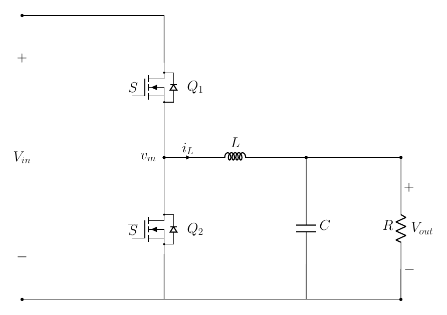
In Chapter 1 we got the headline result, $V_{out} = D\,V_{in}$, by averaging the chopped switch node. That view is quick, but it treats the inductor and capacitor as a black box labelled "filter". In this chapter we open the box and watch the inductor do its work - not with numbers yet, but to build the intuition for why the current looks the way it does. (The numbers and the part-sizing come in Chapter 3.)
What is actually in the box: the four components
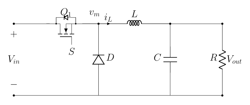
You have already met the whole circuit in Figure 1. Stripped to essentials, it is just two parts:
- the half-bridge - the two switches $Q_1$ and $Q_2$ that take turns chopping the input, from Chapter 1, and
- the L-C filter - an inductor that resists sudden changes in current, followed by a capacitor that resists sudden changes in voltage.
The half-bridge makes the chopped square wave at $v_m$; the L-C filter turns it into smooth DC. The art of the converter is in how the inductor passes energy from input to output, packet by packet.
How the inductor current behaves
The one fact you need about an inductor is its defining law:
$$ v_L = L \, \frac{d i_L}{dt}. $$In words: the voltage across an inductor is proportional to how fast its current is changing. Turn that around and it says something more useful for us - the current is the running total (the integral) of the voltage applied to it:
$$ i_L = \frac{1}{L} \int v_L \, dt. $$So if you put a steady voltage across an inductor, its current ramps in a straight line; flip the voltage negative, and the current ramps back down. The current does not jump - it accumulates.
Now look at our converter. The inductor sits between the switch node $v_m$ on its left and the output $V_{out}$ on its right, so the voltage across it is always $v_L = v_m - V_{out}$. There are two phases (Figure 7):
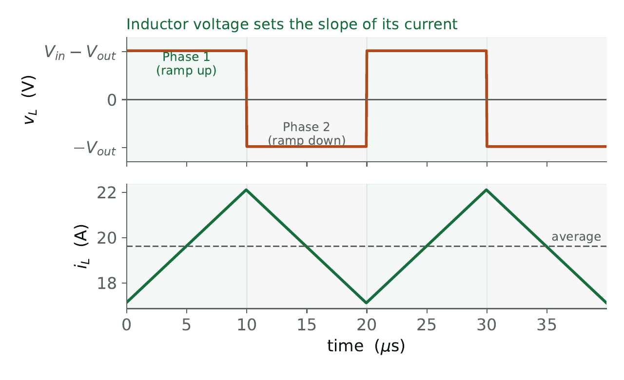
Phase 1 - top switch closed ($v_m = V_{in}$). The inductor sees $v_L = V_{in} - V_{out}$, a positive voltage. Its current ramps up in a straight line - energy flows from the input, through the inductor, into the battery and the capacitor. The inductor is filling up.
Phase 2 - bottom switch closed ($v_m = 0$). Now the inductor sees $v_L = -V_{out}$, a negative voltage. Its current ramps back down, delivering its stored energy onward. The inductor is emptying out.
Fill a little, empty a little, over and over. The current never stops - it just rides up and down by a small amount. That small up-and-down is the ripple, and how big it is, and how you control it, is the whole of Chapter 3.
Where is the energy stored?
Why can the inductor keep pushing current in Phase 2, when the input has been disconnected? Because it has stored energy in its magnetic field. A current flowing through an inductor builds a magnetic field around it, and that field holds an amount of energy
$$ E = \tfrac{1}{2} L \, i_L^2 . $$In Phase 1 the inductor soaks up energy (field grows, current rises); in Phase 2 it gives that energy back (field collapses, current falls), and it is this stored energy that keeps the current flowing into the battery even with the input switched away. The same stored energy is why an inductor "pushes back" against sudden changes - to change its current quickly you would have to change its stored energy quickly, and it resists exactly that.
Think of the inductor as a heavy flywheel for current. The switching tries to yank the current up and down, but the flywheel's stored energy only lets it drift a little each cycle, and keeps it spinning when the drive lets go. A bigger inductor is a heavier flywheel: smoother current, but slower to respond.
Deriving the same result from the inductor volt-second balance
This two-phase picture quietly gives us $V_{out} = D\,V_{in}$ a second time, from a completely different starting point. The argument is worth seeing, because it is the one that leads to ripple and sizing in the next chapter.
In steady state the inductor current must end each cycle exactly where it started - otherwise it would creep away every cycle, which is not a steady state. So whatever the current ramps up in Phase 1, it must ramp back down by the same amount in Phase 2. Since the ramp rate is set by the voltage (the inductor law again), the voltage × time of the two phases must balance:
$$ \underbrace{(V_\text{in} - V_\text{out})\, D\,T_s}_{\text{ramp up, Phase 1}} = \underbrace{V_\text{out}\,(1-D)\,T_s}_{\text{ramp down, Phase 2}}. $$Here $T_s$ is one switching period, so Phase 1 lasts $D\,T_s$ and Phase 2 lasts $(1-D)\,T_s$. Cancel $T_s$, multiply out, and the $V_\text{out}$ terms collect to give, once again,
$$ \boxed{\,V_\text{out} = D \, V_\text{in}\,} $$The inductor's current is the integral of the voltage across it: positive voltage ramps it up (Phase 1), negative voltage ramps it down (Phase 2), and stored magnetic energy carries it between the two. Balancing those two ramps gives the same $V_\text{out} = D\,V_\text{in}$ we found by averaging - and sets us up to measure the ripple.
Designing the filter: choosing L and C
In Chapter 2 we saw how the inductor current behaves - ramping up, then down, every cycle. That up-and-down swing is the ripple, and this chapter is about choosing the inductor $L$ and capacitor $C$ to keep it in check. But before the formulas, the obvious question: why do we care about ripple at all? Two reasons, and they are why nobody just throws in a tiny inductor and calls it done.
Ripple costs you efficiency. The ripple is alternating current, and alternating current is what creates losses in the magnetics and the capacitor. A bigger current ripple swings the inductor's magnetic field harder every cycle, which raises its core loss, and it pushes more alternating current through the output capacitor, which heats it up through its ESR (the small internal resistance every real capacitor has). (Capacitors are even rated for a maximum ripple current for exactly this reason - exceed it and the part overheats and ages early.) So more ripple is not free: it quietly turns into extra heat in the very parts you were trying to keep small. The losses we meet in the next chapter are partly set by the ripple you choose here.
Ripple is noise, and noise is regulated. A converter chopping tens of amps on and off tens of thousands of times a second is, electrically, a little radio transmitter. The switching ripple shows up as electromagnetic interference (EMI) - both conducted out along the input and output wires and radiated into the air - and it can disturb other electronics nearby. This is not optional to care about: almost any product you build and sell has to pass EMC/EMI certification, which sets hard ceilings on how much electrical noise it may emit. Smaller ripple is one of the main levers for staying under those limits, so the ripple target is often dictated as much by what you are allowed to emit as by what the load needs.
Ripple is not just a cosmetic wobble. It turns into heat (extra loss in the inductor and capacitor) and into noise (EMI you must keep below certification limits). That is why ripple is a real design constraint, not an afterthought - and why the cheapest, smallest filter is rarely the right one.
How tight the ripple target needs to be is not something the buck decides on its own - it depends on the system around the converter: how much ripple the neighbouring devices (the battery, the downstream electronics) can tolerate, and the voltage and current limits they impose. Design always starts with those external requirements. With that settled, the rest of the chapter is the how - the two formulas that turn a ripple target into an actual inductor and capacitor.
Sizing the inductor
How big is the ripple? During Phase 1 the inductor sees a fixed voltage $V_\text{in}-V_\text{out}$ for a time $D\,T_s$. Using the inductor law in the form $\Delta i = v\,\Delta t / L$, the peak-to-peak current ripple is
$$ \Delta i_L = \frac{(V_\text{in}-V_\text{out})\,D\,T_s}{L} = \frac{(V_\text{in}-V_\text{out})\,D}{L\,f_{sw}}. $$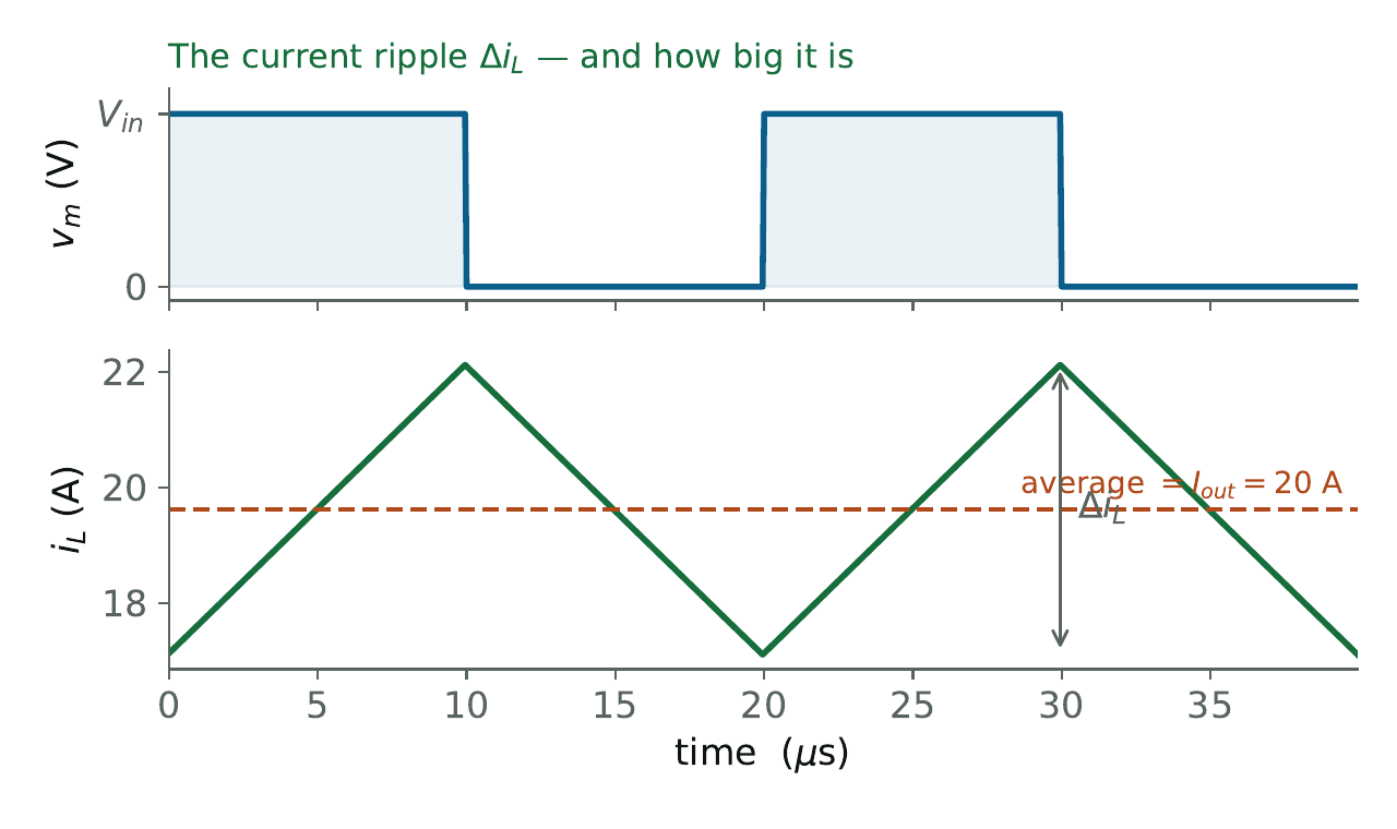
With our numbers - $V_\text{in}=100$ V, $V_\text{out}=50$ V, $D=0.5$, $L=100\ \mu$H, $f_{sw}=50$ kHz:
$$ \Delta i_L = \frac{(100-50)(0.5)}{(100\times10^{-6})(50\times10^3)} = \frac{25}{5} = 5\ \text{A}. $$
So the inductor current swings 5 A peak-to-peak around its 20 A average - from about 17.5 A up to 22.5 A. That is the triangle in Figure 8.
This is the inductor's design equation. The ripple you want is a choice; rearrange for $L$ and you have your inductor:
$$ L = \frac{(V_\text{in}-V_\text{out})\,D}{\Delta i_L \, f_{sw}}. $$Bigger $L$ means smaller ripple, but a physically larger, heavier, more expensive part that responds more slowly to changes. It is always a trade-off.
Notice that the switching frequency $f_{sw}$ sits in the denominator too: the faster you switch, the smaller the ripple. The reason is simple - at a higher frequency each on-time is shorter, so the current has less time to ramp before the switch flips back. Double the switching frequency and you halve the ripple, for the same inductor. (That sounds like a free way to shrink the ripple, but Chapter 4 shows the catch: switching faster costs more loss.)
How much ripple should you aim for? That is a design choice, and it varies a lot from one application to the next. A figure often quoted as a starting point is around 30-40 % of the full load current - but plenty of applications demand far less, and a value that is perfect in one design can be completely wrong in another. Treat any rule of thumb as a starting point to be checked against your requirements, not a law.
The capacitor and the output ripple
The inductor's ripple current has to go somewhere, and the capacitor is what catches it so the battery sees a smooth voltage. The capacitor deserves the same care we gave the inductor - and it behaves as the inductor's exact mirror image.
One thing worth being clear about: the inductor and capacitor together form a simple L-C filter, so the inductor actually affects the voltage ripple too - a bigger $L$ means less current ripple, and less current ripple means less voltage ripple. So why did we size $L$ from the current ripple and leave the voltage ripple to $C$? Because the current ripple is the thing that really matters for the inductor (it sets the peak current and the core loss), and the capacitor has only a small say over it - a bigger $C$ flattens the output voltage a little, which slightly reduces the current ripple. So when you size for current ripple you can safely ignore $C$. The natural division of labour is: pick $L$ for the current ripple, then pick $C$ for the voltage ripple. You could lean on a bigger inductor to shrink the voltage ripple instead, but you usually don't, because that is the capacitor's cheaper job.
Where the inductor's law was "voltage sets the rate of change of current", the capacitor's law is the reverse:
$$ i_C = C \, \frac{d v_C}{dt} \qquad\Longleftrightarrow\qquad v_C = \frac{1}{C}\int i_C\,dt. $$In words: the current into a capacitor sets how fast its voltage changes, so the capacitor voltage is the running total (integral) of the current poured into it. Inductor: current is the integral of voltage. Capacitor: voltage is the integral of current. A neat duality.
Now, which current flows into the capacitor? Look at the output node, where three wires meet (Figure 9): the current $i_L$ arriving from the inductor, the current $i_R$ leaving into the load, and the current $i_C$ going into the capacitor. Kirchhoff's current law says what arrives must leave:
$$ i_C = i_L - i_R. $$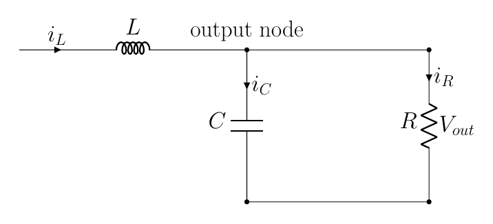
Here is the key simplification. The output voltage ripple is tiny compared with $V_{out}$ - millivolts on tens of volts - so for the purpose of the load, the output is essentially constant, and the load current $i_R \approx I_{out}$ is steady DC. The inductor current, meanwhile, is its average ($I_{out}$) plus the triangular ripple. Subtract the steady part and what is left - the ripple - has nowhere to go but into the capacitor:
$$ i_C = i_L - I_{out} = \text{the ripple triangle, swinging } \pm\tfrac{\Delta i_L}{2}. $$So the capacitor current is a triangle centred on zero, half the inductor's peak-to-peak ripple in each direction. And since the capacitor voltage is the integral of that current, the output ripple is the running total of this triangle (Figure 10): the voltage rises while $i_C$ is positive (capacitor charging) and falls while $i_C$ is negative (discharging), lagging the current by a quarter cycle.
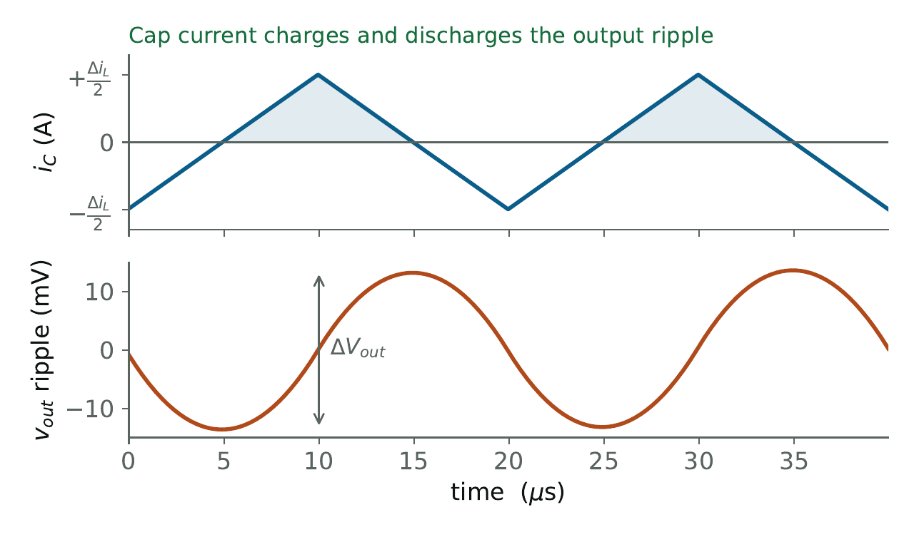
Integrating that triangle over the half-cycle it is positive gives the charge delivered to the capacitor, $\Delta Q = \tfrac12 \cdot \tfrac{T_s}{2} \cdot \tfrac{\Delta i_L}{2}$, and a charge $\Delta Q$ on a capacitor $C$ raises its voltage by $\Delta Q / C$. Working it through gives the output-ripple formula:
$$ \Delta V_\text{out} = \frac{\Delta i_L}{8\,C\,f_{sw}}. $$With $\Delta i_L = 5$ A, $C = 470\ \mu$F, $f_{sw} = 50$ kHz:
$$ \Delta V_\text{out} = \frac{5}{8(470\times10^{-6})(50\times10^3)} = \frac{5}{188} \approx 27\ \text{mV}. $$
On a 50 V output that is about 0.05 % - invisible to the battery. That is the capacitor doing its job, and it tells you how to size it: pick the ripple voltage you will accept and solve for $C$.
One caveat the clean formula hides: a real capacitor has a small internal resistance, its ESR (equivalent series resistance). The ripple current flowing through the ESR makes its own little voltage, $\Delta i_L \times \text{ESR}$, which often dominates the real output ripple. This is why datasheets obsess over low-ESR capacitors - and it comes back to bite us in the control chapters.
When the current hits zero: CCM and DCM
Everything so far assumed the inductor current stays positive. But the average current is set by the load, and as you lighten the load that average slides down while the triangle keeps its size. Eventually the bottom of the triangle reaches zero. What happens next depends entirely on the bottom device - and this is exactly where the diode-versus-switch choice matters (Figure 11).
A diode only allows current in one direction - it physically blocks any reverse flow. So in the diode buck, when the inductor current tries to go negative, it simply can't: the diode stops conducting, and the current sits flat at zero until the next cycle begins. That is discontinuous conduction mode (DCM). A synchronous buck, by contrast, has a transistor there that conducts both ways, so the current is free to swing negative and the converter stays in continuous conduction mode (CCM) at any load. Figure 12 shows the two side by side.
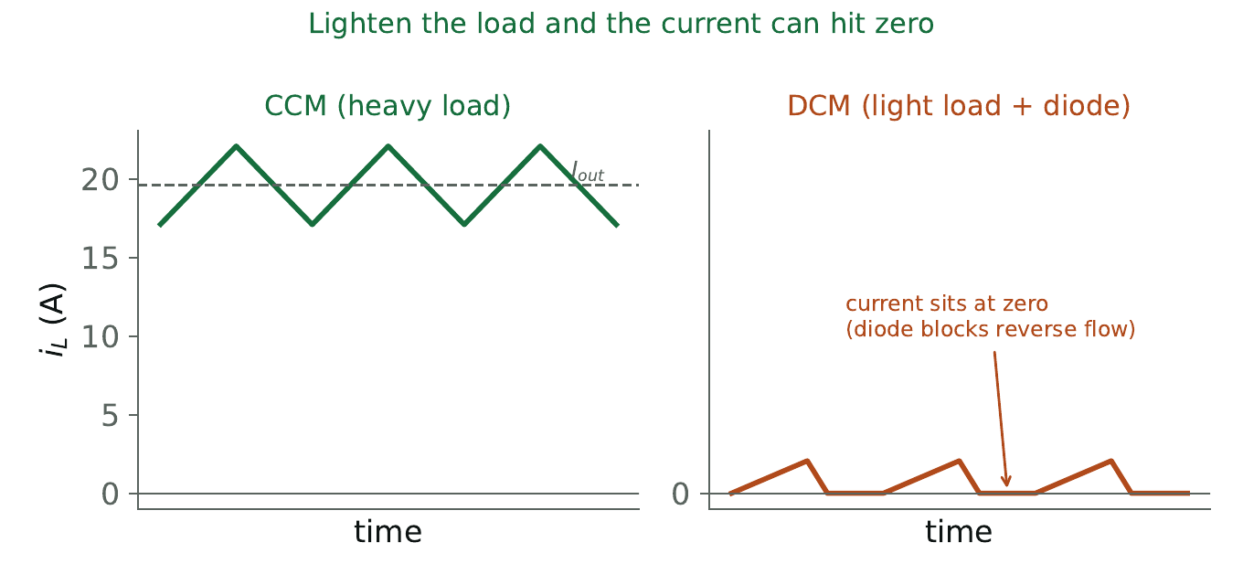
In continuous conduction mode the inductor current never reaches zero. In discontinuous mode it does, and rests at zero for part of the cycle. The boundary is where the load current equals half the ripple, $I_{out} = \Delta i_L / 2$. In DCM the simple rule $V_\text{out} = D\,V_\text{in}$ no longer holds - the output then also depends on the load.
Design is about two formulas. Size the inductor from the current ripple you'll accept, $\Delta i_L = (V_\text{in}-V_\text{out})D/(Lf_{sw})$; size the capacitor (and mind its ESR) from the voltage ripple, $\Delta V_\text{out} = \Delta i_L/(8Cf_{sw})$. And remember that at light enough load a diode-based buck slips into DCM, where the current rests at zero.
Where the energy goes
A real buck is not 100 % efficient - it is just very good. But before we open up where the missing few percent go, it is worth being clear on why we care so much, because the answer is not what most people assume.
It is tempting to think efficiency is just about the energy you waste - a 97 % converter throws away 3 % of the power, and that is that. But the wasted power does not vanish; it turns into heat, right there inside the converter. And that heat is the real problem.
Every component has a temperature it can tolerate, and no more. A MOSFET has a maximum junction temperature; push past it and it degrades or fails. The inductor's core loses its magnetic properties when it gets too hot, and its winding insulation cooks. Electrolytic capacitors dry out and age dramatically faster the hotter they run. So the losses are not just an electricity bill - they are heat you are obliged to get out of the converter before it damages itself.
That reframes the whole point of efficiency. In our 1 kW converter, going from 97 % to 94 % efficient doubles the wasted power from about 30 W to 60 W - and now you have twice as much heat to deal with. You are then left with three ways to spend money: buy beefier, higher-temperature-rated components that can survive the heat; add cooling (bigger heatsinks, a fan) to carry it away; or invest in making the converter more efficient in the first place so the heat is never produced. Efficiency is really a choice about which of those costs you pay.
Lost power is not just lost money - it is heat inside the box. Every part (MOSFET, inductor, capacitor) has a temperature limit, and exceeding it shortens its life or destroys it. So higher efficiency buys you a cooler, more reliable, often cheaper converter - because you need less cooling and less over-rated hardware. That is why engineers chase those last percent so hard.
So this chapter opens up the small fraction of power that does not reach the battery - because that lost power is heat, and heat is what decides how you cool the converter, how big the parts must be, and how long it lasts.
Three families of loss
Every loss in a buck falls into one of three buckets, and the differences between them explain the whole efficiency story.
- Conduction loss - the price of carrying current. Current flowing through a transistor's on-resistance $R_{ds(on)}$, and through the inductor's winding resistance (its DCR), burns $I^2 R$. It grows with the square of the load current.
- Switching loss - the price of changing state. Every time a transistor turns on or off there is a brief moment when it has both voltage across it and current through it, and that overlap burns energy. Charging the gate and the device's capacitances costs a fixed sip each cycle too. All of it is paid per switching cycle, so it grows with frequency but barely cares about the load.
- Magnetic (core) loss - the price of cycling the inductor's core. Every cycle, the magnetic field in the core is built up and torn down, and the core material resists that (hysteresis), while small induced eddy currents swirl inside it. This heats the core whether the load is heavy or light, and it grows with frequency and with how hard you swing the magnetic field. With a cheap core it can be surprisingly large.
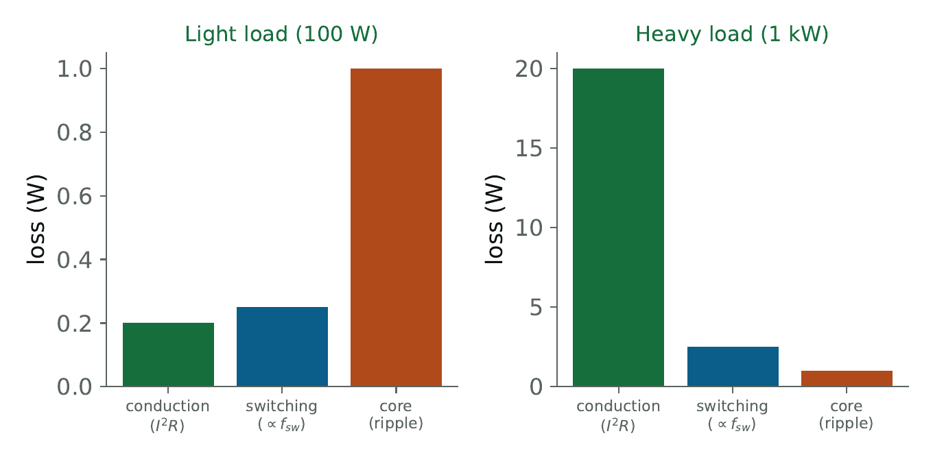
Two analogies. Conduction loss is friction - it grows the harder you push (more load current). Switching loss is a toll - the same whether your truck is full or empty, paid every time you cross the bridge (every cycle). And core loss is the flywheel warming up from being flexed back and forth each cycle, regardless of what it is driving. At light load the tolls and the warm flywheel dominate; at heavy load the friction does.
It helps to know what each loss actually depends on, because that is what tells you which knob changes which loss. For the curious, here are the simplest forms (each is an approximation - real life is messier, especially the core loss):
- Conduction depends on current and resistance: $P_\text{cond} = I^2 R$. Nothing you can do about the current (the load sets it), so you fight this with lower-resistance parts.
- Switching depends on the switching frequency: each on/off transition wastes a fixed packet of energy, so $P_\text{sw} \approx \tfrac{1}{2}\,V_\text{in}\,I\,(t_r + t_f)\,f_{sw}$ - double the frequency, double this loss.
- Core (magnetic) is genuinely complex - it depends on the core material, the frequency, and the detailed shape of the magnetic cycling, and the full description (the Steinmetz equation) raises more questions than it answers. But on a surface level the one thing worth holding onto is simple: there is a positive relationship between the current ripple and the core loss. The more ripple you push through the inductor, the more its core heats up - and the loss climbs with switching frequency on top of that. (Cheap core materials simply lose more for the same ripple.)
Notice that two of the three losses grow with the switching frequency $f_{sw}$. This is the catch behind a tempting idea: back in Chapter 3 the ripple shrank as $1/f_{sw}$, so why not just crank the frequency sky-high and make the ripple vanish? Because the switching and core losses go the other way - up with frequency. The switching frequency is therefore a genuine trade-off: high enough for small ripple and small magnetics, low enough to keep the losses (and heat) manageable. There is no free lunch at $f_{sw} = \infty$.
The efficiency curve
Put those together and you get the characteristic efficiency curve every buck datasheet shows (Figure 13). At very light load the delivered power is tiny but you are still paying the fixed switching and core losses every cycle, so efficiency is poor. As load rises those fixed costs are spread over more delivered power and efficiency climbs to a peak. Push the load higher still and the $I^2R$ friction takes over, dragging efficiency back down.
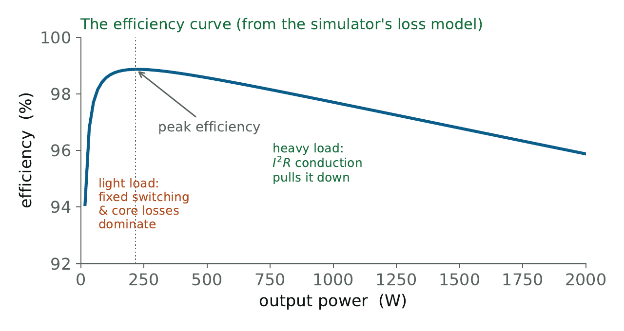
Figure 14 shows the same story as a loss budget at two operating points. At light load the bars are mostly switching and core; at heavy load conduction towers over everything else.
These three families are the big ones, but they are not the whole list. A real converter also burns a little power on housekeeping - the controller and its firmware, the gate drivers, the voltage references and sensing, all drawing a small steady current whether or not you are delivering any load. And if the design needs active cooling, the fan itself costs power. None of these usually dominate, but they are why a real efficiency number never quite reaches the figure the three families alone would predict - especially at very light load, where the fixed housekeeping draw is competing with very little delivered power.
Why pay for the second switch?
Now we can settle the synchronous-versus-diode question. The diode buck (Figure 6, back in Chapter 1) is cheaper and needs no gate drive, but the diode has a stubborn problem: while it conducts it drops a forward voltage $V_F$ of perhaps 0.4-0.7 V, and all the load current flows through that drop. At 20 A and $V_F = 0.5$ V, during the half of the time the diode conducts, that is roughly 5 W wasted - and it scales straight up with current. A synchronous MOSFET instead drops only $I \times R_{ds(on)}$, which for a milliohm-class device is far smaller. That is why high-current converters pay for the second switch: at heavy load the MOSFET's tiny $I R_{ds(on)}$ beats the diode's fixed $V_F$ handily.
The twist is at light load, where keeping the synchronous switch on lets current flow backwards and wastes energy circulating it. So good controllers make the bottom MOSFET act like a diode at light load - diode-emulation, turning it off when the current reaches zero (back into DCM). That is the best of both worlds, and it is why a good charge controller stays efficient whether the sun is blazing or barely up.
A switch also conducts both ways, where a diode conducts only one, so a two-switch converter can be bidirectional - useful for a battery that must both charge and discharge. But if you only ever run one direction (our solar charge controller only charges), you don't need that, and a cheaper unidirectional part - a diode, or a simple switch - is perfectly fine.
Losses come in three families: conduction ($I^2R$, friction, grows with load), switching (a per-cycle toll), and magnetic core loss (the inductor heating up, worse with cheap cores). Their balance sets the efficiency curve's peak. Synchronous MOSFETs win at heavy load; diode-like behaviour wins at light load - so good converters do both.
Controlling a buck: an overview
Up to now we have set the duty cycle $D$ by hand. From here on a controller sets it automatically, moment to moment. This chapter is the map: what we choose to control, and why. The detailed how - the actual controllers - comes in the chapters after.
What you control depends on the system around it
A buck never sits alone. It sits between a source on its input and a load on its output. In our running example the source is the solar string and the load is the battery. That surrounding system decides what we control.
Source (solar panel) → Buck converter + controller → Load (battery), with a feedback path from the buck's output back into its controller. The source hands the buck a voltage; the controller steers the output the load needs.
The input side is essentially fixed - the source hands us a voltage we do not get to choose (and which drifts as the sun and temperature change). What we can steer is the output. For a buck that almost always means we control the output voltage: we want a steady voltage for the battery, no matter how the input or the load wanders.
In some converters you would instead control the power - when the job is to push a set amount of power rather than hold a voltage (common for grid inverters). For a buck it is almost always voltage, because that is what the downstream device needs, and it is the simplest thing to regulate. So voltage is what we will control.
The voltage loop, previewed
To hold the output voltage, the controller does the obvious thing: it looks at the output, compares it to the target $V_{ref}$ (which the MPPT or charge logic asks for), and adjusts the duty cycle to close the gap - output too low, push $D$ up; too high, ease it down. To do that, the controller has to know the output voltage. The simplest way is just to measure it, which is what we will assume throughout. (You do not strictly have to measure it - it is also possible to estimate the output from other quantities, so-called sensorless control - but that usually costs you accuracy or computation, so a direct measurement is the normal choice.) That is the voltage controller, sketched below.
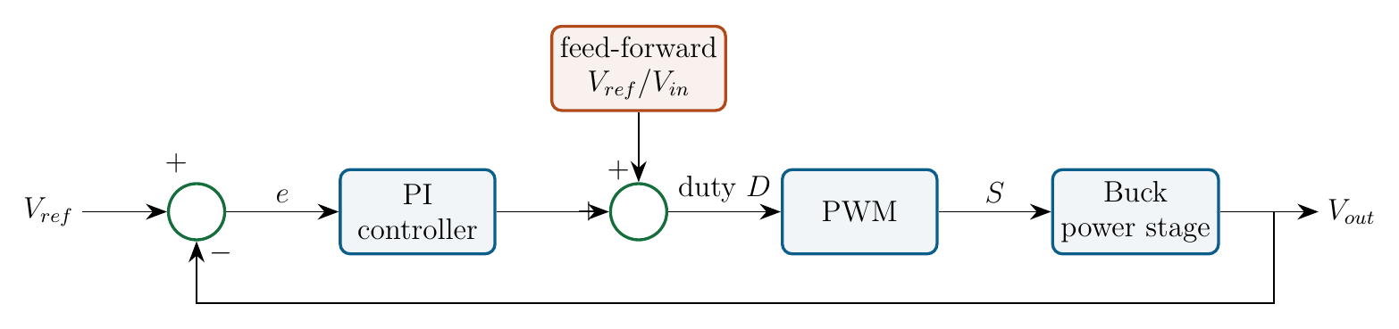
For many buck converters, that is the whole story - one loop, holding the voltage.
Why also control the current
A voltage-only controller has one blind spot: it cares only about the voltage, and lets the current do whatever that requires. Most of the time that is fine. But during a big disturbance - a sudden jump in the reference, or a load step - the controller may demand a large change in voltage, and the inductor current can surge to whatever value delivers it. Large currents are bad news on their own: more current means more loss, which means more heat, which is what eventually damages the switches and the battery (Chapter 4). So we want to keep the current in check.
(Worth knowing: a real converter also has a separate, fast hardware protection that trips on a dangerous current spike all by itself - we come back to that in Chapter 8. What we are about to add is the controller's own handle on the current.)
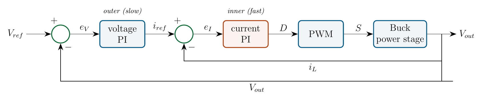
So in many designs we add a second, inner loop that controls the inductor current directly. The outer voltage loop no longer sets the duty itself - it asks for a current (a target $i_{ref}$), and the inner loop makes the current follow it. This nesting is cascade control (sketched below), and its decisive advantage is that you can simply cap the current target: the converter then physically cannot exceed a safe current, however hard it is pushed.
Voltage, current, or both?
So "what do you control?" has two answers, and which you pick is a property of the system, not the converter:
- Voltage only - the simplest choice, and enough when nothing bad happens if the current does whatever it likes.
- Voltage and current (cascade) - when you must keep the current in check: avoid spikes, limit inrush, protect the battery and the switches.
Neither alone is the full picture: voltage control sets the output the load needs, but does not protect the hardware; current control protects the hardware, but on its own does not set the output. Cascade gives you both, which is why it is the workhorse - and why we build up to it.
The gap between duty cycle and gate signal
There is one piece still missing. Both controllers output a duty cycle - a number between 0 and 1. But the switches only understand on and off. The bridge between the controller's duty cycle and the actual gate signal is PWM, and it is where we go next.
Control of a buck comes down to what you steer and why. The input is fixed by the source, so we steer the output voltage for the load. If the current must also be kept safe, we add an inner current loop - cascade control - which lets us cap the current. Voltage for the load, current for protection; the system decides whether you need one loop or both.
PWM: turning a duty cycle into gate signals
The controller's whole job, as we will see, is to compute one number: the duty cycle $D$. But the switches do not understand a number like "$0.5$" - they only understand on or off. Pulse-width modulation (PWM) is the small piece that bridges the two: it turns a duty-cycle number into the on/off gate signal $S$ that actually drives the switch.
Why not just control the switch directly?
You might ask why we bother with a duty cycle at all - why not have the controller flip the switch on and off itself? Because a duty cycle is an easy thing to control, and a gate signal is not.
The duty cycle is a smooth, continuous number: it can take any value between 0 and 1, and a controller can nudge it by a hair - from $0.500$ to $0.501$ - to make a tiny correction. The gate signal is the opposite: it is binary, fully on or fully off at every instant, with nothing in between. Controlling that on/off pattern directly is clumsy - to place a switching edge with any precision you would have to decide the switch state extremely often, far faster than the switching itself, just to get fine resolution.
So we split the problem in two. The controller lives in the easy, continuous world of the duty cycle (that is what all the control chapters that follow are about), and one dedicated block - PWM - does the single job of turning that smooth number into the binary pattern the switches need.
A duty cycle is an average
Remember from Chapter 1 that the duty cycle is just the average of the gate signal over a switching period - the fraction of the time the switch is on. So PWM has a simple target: produce a gate signal $S$ that is on for a fraction $D$ of every period.
The standard way to do it sounds more complicated than it is, so do not worry if the next sentence does not click immediately - the plot just below makes it obvious. Generate a triangular carrier that ramps from 0 up to 1 and back down to 0, exactly once per switching period - so the carrier's frequency is the switching frequency $f_{sw}$ - and compare it against the duty cycle:
$$ S = \begin{cases} 1 & \text{if } D > \text{carrier} \\ 0 & \text{otherwise.} \end{cases} $$That comparison is the entire PWM block (Figure below): two inputs - the duty from the controller and the carrier - and one output, the gate $S$.
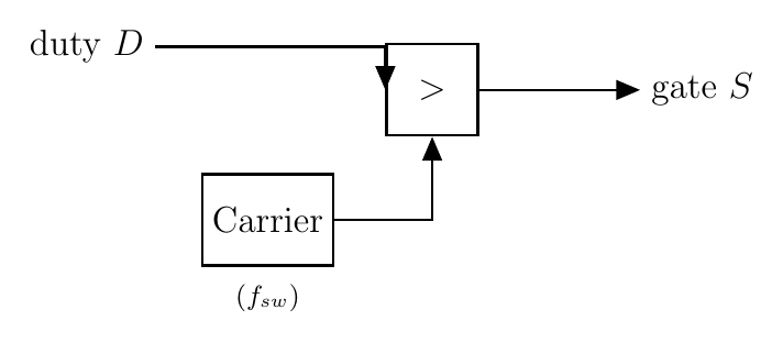
When $D$ is large, it sits above the carrier for most of the period, so $S$ is on most of the time. When $D$ is small, the carrier pokes above it for most of the period and $S$ is mostly off. The waveform below shows it for $D = 0.5$: the gate is on for exactly half of each period.
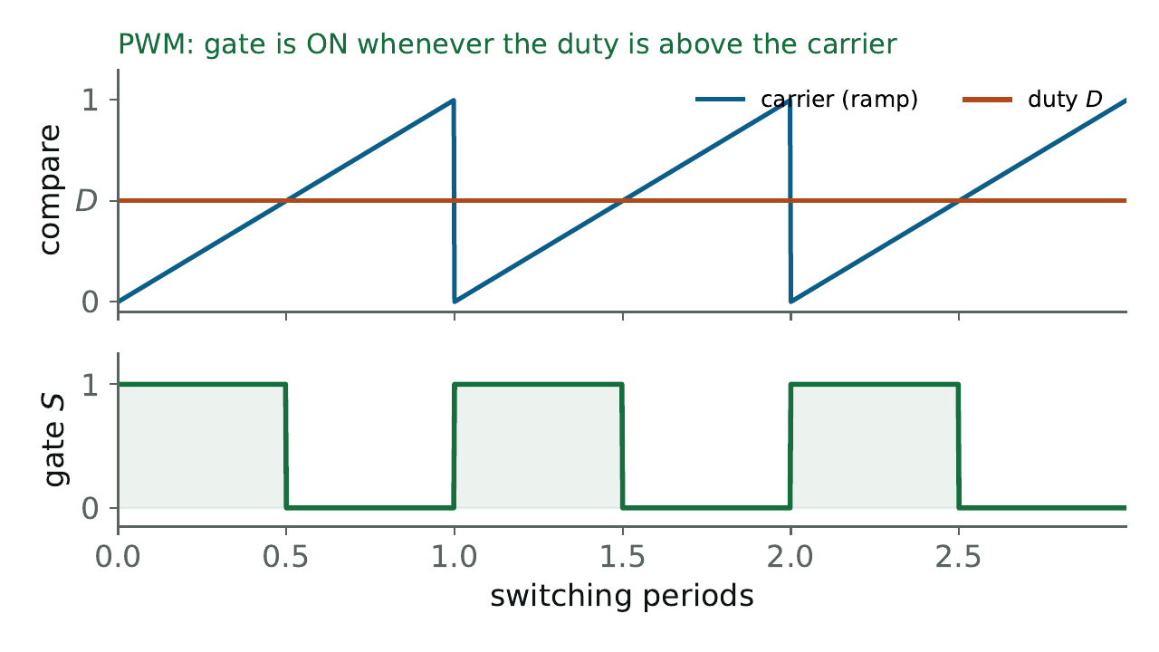
PWM is the translator. Everything upstream - the controller - just decides what duty cycle to ask for. PWM turns that number into the actual on/off switching pattern, period after period. Change the switching frequency and you change the carrier's frequency, nothing else.
PWM is an analog process. The comparison "is the duty above the carrier?" happens continuously, in real time - classically a simple analog comparator, running every instant. That is different from the controller, which is usually a digital calculation updated at discrete sample instants. So while the controller takes a fresh look only every so often, the PWM that follows it reacts instantly and continuously. (This is also why we draw PWM as its own block, separate from the controller.)
In code it is exactly the one-liner the comparison describes - this is the PWM block you will find in the simulator:
// PWM: compare the duty against a triangular carrier in [0,1].
int pwm_step(float duty, float carrier) {
    int S = (carrier < duty) ? 1 : 0;   // upper switch on while duty > carrier
    return S;                           // lower switch takes the complement
}The controller outputs a duty cycle; PWM converts it to gate pulses by comparing it against a triangular carrier - $S$ is on whenever $D$ is above the carrier. From here on, "the controller sets $D$" and "PWM makes the switches obey" are two separate jobs.
Controlling the voltage
Now we open up the voltage controller from the overview. We build it in two steps: first a model that predicts the right duty cycle, then a PI that corrects for everything the model cannot capture. The structure is the one sketched in Chapter 5, repeated below.
Step 1: the model (feed-forward)
We already have a model of the converter - the rule from Chapter 1. Inverting $V_{out} = D\,V_{in}$ tells us the duty that should produce the voltage we want:
$$ D_{ff} = \frac{V_{ref}}{V_{in}}. $$This is the feed-forward: a duty we compute straight from the model, before measuring anything. If the converter were ideal and we knew $V_{in}$ exactly, this would be the entire controller - set $D = V_{ref}/V_{in}$ and the output sits at $V_{ref}$ ($50/100 = 0.5$, with our numbers). It is the best we can do from prediction alone.
Step 2: the PI (correcting what the model misses)
But the model is never the whole truth. We do not capture the losses exactly; $V_{in}$ is measured with some error; there is electrical noise; and the components themselves drift - the inductance changes with current and temperature, the capacitance ages, and there are always small effects we never wrote into the equation at all. The feed-forward cannot know about any of this.
So we measure the actual output, form the error $e = V_{ref} - V_{out}$, and add a PI correction on top of the feed-forward:
$$ D = \underbrace{\frac{V_{ref}}{V_{in}}}_{\text{model (feed-forward)}} \;+\; \underbrace{K_p\, e \;+\; K_i\!\int e\,dt}_{\text{PI: corrects the rest}}. $$The PI is precisely the part that handles what the model left out. The proportional term ($K_p\,e$) reacts to the error right now; the integral term ($K_i\!\int e\,dt$) accumulates it, so that even a small, stubborn error - exactly the kind that drift and unmodelled losses produce - is eventually driven to zero.
Read the controller as model plus humility. The feed-forward is our best guess from the equations; the PI quietly admits the equations are never perfect and mops up the difference - the noise, the parameter drift, the things we didn't model. That is also why we measure the output at all: to control the voltage you must know it, and the measurement is what lets the PI catch everything the model can't.
Step response of the voltage loop
The figure below shows this controller handling a step up in the reference voltage. The output is driven cleanly to its new target. Now look at the bottom trace: while the voltage is being controlled, the current simply does whatever the voltage demands - here it surges well past the steady value before settling. The voltage controller never looks at the current. Most of the time that is harmless; sometimes, as the next chapter shows, it is not.
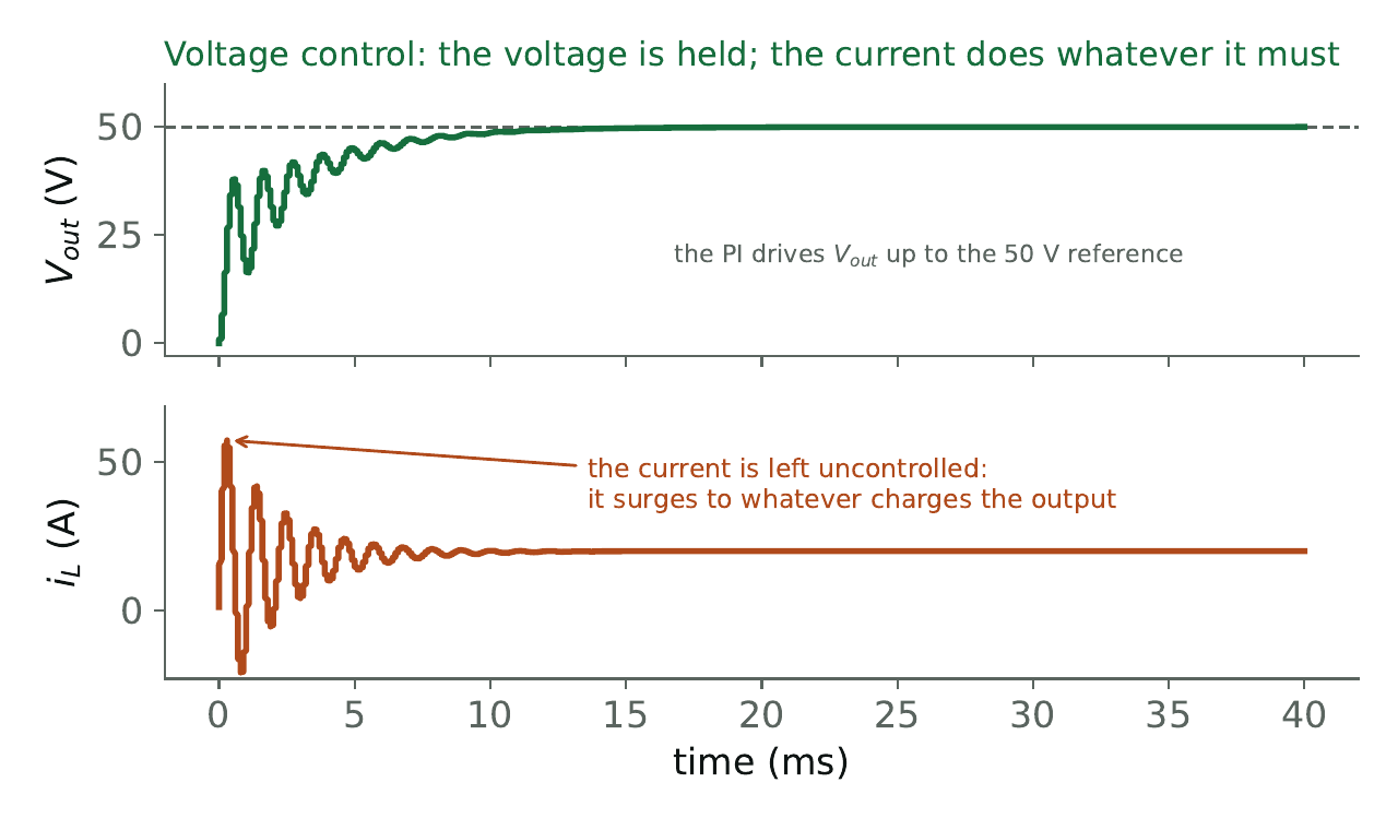
We won't go into tuning the gains $K_p$ and $K_i$ here - that is the same story for every converter and belongs to control theory, not power electronics. The short version: more $K_i$ removes error faster but rings if overdone; more $K_p$ is snappier but jittery if overdone. The honest way to find them is to try, which is what the simulator is for.
A voltage controller is a model plus a corrector: the feed-forward $V_{ref}/V_{in}$ predicts the duty from the equation, and the PI corrects for everything the equation misses - noise, parameter drift, unmodelled losses - by acting on the measured output. It holds the voltage; it does not watch the current.
Cascade control: voltage outside, current inside
The single voltage loop works. But almost every serious converter - and the default controller in the simulator - uses a smarter arrangement: cascade control, with two nested loops. It is the standard way to control a buck, and it is worth understanding why.
The idea is to control the inductor current directly with a fast inner loop, and let a slower outer loop decide how much current to ask for. The structure is the one from Chapter 5, repeated below.
Two loops, two jobs
Outer loop - voltage. It looks at the output error $e_V = V_{ref} - V_{out}$ and, instead of a duty cycle, produces a current reference $i_{ref}$ - its way of saying "to fix this voltage error, the inductor should carry this much current." Here the model has little to add, so a PI does the work:
$$ i_{ref} = K_{p,V}\, e_V + K_{i,V}\!\int e_V\, dt. $$Inner loop - current. This is where the model-plus-corrector idea from the last chapter returns in full. We want the inductor current to follow $i_{ref}$. From the converter's behaviour, the duty that holds a steady operating point is $D_{ff} = V_{out}/V_{in}$ (the same relation as before, now using the measured output) - that is the model for the current loop. On top of it, a PI corrects the current error $e_I = i_{ref} - i_L$ and everything the model misses:
$$ D = \underbrace{\frac{V_{out}}{V_{in}}}_{\text{model (feed-forward)}} \;+\; \underbrace{K_{p,I}\, e_I + K_{i,I}\!\int e_I\, dt}_{\text{PI: corrects the rest}}. $$So the inner loop is built the way we built the voltage controller in the last chapter - a model plus a PI corrector - while the outer loop is a PI alone. That asymmetry is the point: the feed-forward belongs in the fast loop, where it has something to gain, and the slow loop does without it. In practice it matters a great deal here: without the feed-forward the current loop is sluggish and overshoots, and with it the current tracks its reference cleanly.
Keep the loops at different speeds
There is one rule about cascade control you cannot skip: the inner current loop must run faster (have a higher bandwidth) than the outer voltage loop. This is not just a nicety - it is what keeps the two loops from fighting each other.
The reason is interference. If the two loops responded at the same speed, they would both react to the same disturbance at the same instant, each one partly undoing the other's correction. The result is a tug-of-war that shows up as oscillation. The cure is separation: make the inner loop several times faster, so the current has already settled before the voltage loop even notices the disturbance. The voltage loop then sees a current that simply does what it asks - clean and already handled - and the two cooperate instead of interfere.
The golden rule of cascade control: inner loop fast, outer loop slow. The current loop must be clearly faster than the voltage loop, or the two interfere and the converter oscillates. How much faster (and the exact gains) is control-theory tuning - not our focus - but the separation itself is non-negotiable.
Why bother with two loops?
Three reasons, all practical:
- The inner loop tames the inductor. By forcing the current to follow a command, the fast current loop hides the inductor's dynamics from the outer loop. The voltage loop no longer "sees" a tricky $L$-$C$ system - it just sees something that delivers whatever current it asks for. That makes the outer loop much easier to get right.
- Current limiting comes for free. This is the big one. Because the outer loop's output is the current command, you can simply clamp $i_{ref}$ to a maximum, and the converter then holds the inductor current at that value - it cannot drive a sustained current past the limit (the current may overshoot it briefly on a fast transient, since the inner loop has finite speed, but it cannot hold above it). That protects the switches, the inductor, and (in our solar example) the battery, which must not be charged too hard. Doing this with a plain voltage loop is clumsy; with cascade it is one line.
- Faster, cleaner response to disturbances, because the inner loop reacts to current changes immediately rather than waiting for them to show up as a voltage error.
You may hear this called current-mode control in industry - it is the same idea, and it is what most commercial buck regulator chips use, precisely for the easy current limiting and the well-behaved outer loop. The single voltage loop of the last chapter is voltage-mode control. Cascade/current-mode is the workhorse.
Two kinds of current limit: software and hardware
The current limit we just described lives in the controller - it is software clamping $i_{ref}$. But there is almost always a second current limit built into the hardware itself, and the two protect against different things.
The software limit (the clamp on $i_{ref}$) guards against sustained over-current: the load draws too much, or the reference is set too high, and the controller simply refuses to command more than the safe value. It shapes the current during normal operation, where "normal" includes things going a bit wrong for a while. But software is far too slow to catch a sudden spike - a short on the output, or a fault transient, can shoot the current up and be gone in a microsecond, long before the control loop takes its next look. Those are caught by a hardware limiter: a fast analog comparator (often a cycle-by-cycle current limit built into the chip) that shuts the switch off the instant the current crosses a threshold, reacting in around a hundred nanoseconds with no software in the loop. If the fault persists, the hardware escalates on its own - retrying in "hiccups" or latching off entirely.
A real converter usually has both limits. The hardware limiter is fast and protects against current spikes (surges, faults) that software could never react to in time. The software limiter (the $i_{ref}$ clamp) is what shapes the sustained current during normal operation. A plain voltage-mode converter can still have the hardware limiter for protection; what cascade control adds is the clean software limit on top.
Step response with the current loop inside
The figure below shows the startup of the same converter, now under cascade control. The voltage still rises to its target - but look at the current. Instead of surging freely to 57 A as it did under voltage control, it is held close to a limit we set: the outer loop asked for far more current than that, but because its command is a current, we simply capped it.
One detail is worth pointing out, because you will notice it the moment you run this and people always ask about it: the inductor current peaks a little above the 30 A limit line. That is not a mistake. We do not clamp the current itself - we clamp the current reference $i_{ref}$, and the inner loop then drives the real current $i_L$ to follow that reference. Like any control loop it has finite speed, so during the fast startup the current overshoots its reference slightly before the loop catches it. The reference is held exactly at the limit; the current tracks it with a small, normal control overshoot. (Want it tighter? Tune the inner loop faster, or lower the limit a touch to leave margin - it is a tuning choice, not a flaw.) Same converter, same startup as the voltage-only case - but now the current is firmly in hand instead of surging to nearly three times the load.
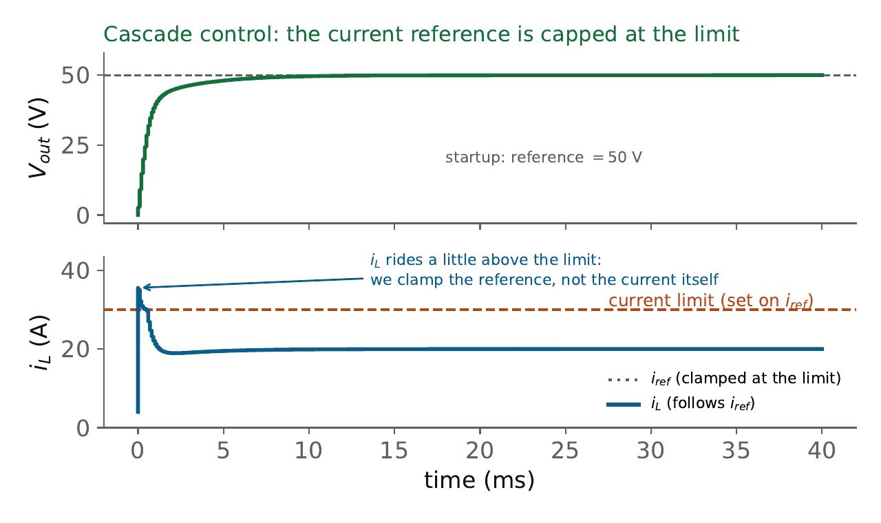
Cascade control nests a fast inner current loop inside a slower outer voltage loop: the voltage loop commands a current ($i_{ref}$), the current loop delivers it (by setting $D$). It tames the inductor, gives effortless current limiting, and responds faster - which is why it is the standard buck controller, in textbooks and in silicon alike.
Where to go next
You now have the whole arc: why we step DC down by chopping and averaging, how the inductor and capacitor behave and how to size them, where the losses go, and how to control the output - from PWM, to a single voltage loop with feed-forward, to the cascade of voltage and current loops that real converters use.
And here is the nice part: every block diagram in these last chapters is implemented for real in the companion simulator, running against a real switched model of the converter. So the best next step is to play. Run the voltage controller, then the cascade; step the load, clamp the current and watch it protect itself; change the gains and feel the response. Every idea in this book has a knob in there waiting for you.
When you are ready for the mirror image of the buck - the converter that steps voltage up, the one that does solar MPPT from the other side - the boost converter guide picks up exactly where this one leaves off.